My own instruction set with an assembler and emulator, a CPU drawn gate by gate in Logisim that runs the same bytecode, and the arithmetic core built again on a breadboard with real ICs.
The C# emulator ported to JavaScript so it runs here. Left is the assembly; right is the assembled 32-bit words, the registers (a box lights up when an instruction writes it), RAM 0–15 and the console. Click the console and type to feed READ.
One bytecode, three machines
In this project, I made three separate but related systems: an assembler -> disassembler -> emulator toolchain, a Logisim simulation, and a breadboard ALU, all built around the same ISA spec sheet that I defined here.
The emulator has the most robust implementation of my ISA, while the Logisim simulation and the physical buildout both implement a subset of the full set of instructions.
SimpleISA
Every instruction is one 32-bit word, [OPCODE | P1 | P2 | P3]. Each opcode fixes what its three slots mean (register, immediate, jump target or padding), so decoding is just a table lookup. 40 08 05 00 is SET R0 5. There are 32 registers: eight special ones (ZERO, ONE, CHAR, FLAGS, RNDM, USER, IP and a spare) and R0–R15.
Category
Mnemonic
Opcode
Operands
Notes
None
NONEhardware
0x00
-
No-op for one cycle. Also what the assembler's trailing padding words decode to.
Math
ADDhardware
0x10
out R1 R2
out = R1 + R2
Math
SUBhardware
0x11
out R1 R2
out = R1 − R2, wraps (0 − 1 = 65535 in the emulator)
Math
MULThardware
0x12
out R1 R2
Math
DIVhardware
0x13
out R1 R2
Integer division; ÷0 gives 0
Math
LSHFhardware
0x14
out R1
Shift left one bit (in the ALU)
Math
RSHFhardware
0x15
out R1
Shift right one bit (in the ALU)
Math
GTHANhardware
0x16
out R1 R2
out = 1 if R1 > R2, else 0
Math
EQhardware
0x17
out R1 R2
out = 1 if R1 = R2, else 0
Math
LTHANhardware
0x18
out R1 R2
out = 1 if R1 < R2, else 0
Math
SETBITemulator
0x19
out bit
Set bit bit of out (0 = LSB)
Math
CLRBITemulator
0x1A
out bit
Clear bit bit of out
Logic
NOThardware
0x20
out R1
Logic
ANDhardware
0x21
out R1 R2
Logic
ORhardware
0x22
out R1 R2
Logic
NORhardware
0x23
out R1 R2
Logic
NANDhardware
0x24
out R1 R2
Logic
XORhardware
0x25
out R1 R2
Logic
RSHFVARhardware
0x26
out R1 R2
Shift R1 right by R2 bits
Flow
JMPhardware
0x30
label
IP = label (an instruction index)
Flow
JMPZhardware
0x31
label R1
Jump if R1 = 0
Flow
JMPEQhardware
0x32
label R1 R2
Jump if R1 = R2
Memory
SEThardware
0x40
R1 val
R1 = immediate 0–255
Memory
MOVhardware
0x41
out R1
Destination first: MOV R0 R1 copies R1 into R0
Memory
LOADhardware
0x42
out addr
out = RAM[addr]
Memory
STRhardware
0x43
R1 addr
RAM[addr] = R1
Memory
POPspec only
0x44
R1
Reserved for the stack (not yet in the assembler or emulator)
Memory
PUSHspec only
0x45
R1
Reserved for the stack
Memory
PRNTemulator
0x46
-
If FLAGS bit 0 is set: clear it and print CHAR
Memory
READemulator
0x47
-
If a key is waiting: CHAR = key, set FLAGS bit 1. Non-blocking, so programs poll.
Memory
INCemulator
0x48
R1
R1 += 1
Memory
DECemulator
0x49
R1
R1 −= 1
Memory
RNDMemulator
0x4A
min max
If FLAGS bit 2 is set: clear it, RNDM = random in [min, max)
The 24 marked hardware run on the Logisim CPU, the rest only exist in the emulator. Note that the toolchain numbers the general registers from 0x08 and the Logisim ROM images number them from 0x00, so the same SET R0 5 is 40000500 there.
Here it is running count_to_five from ROM, slowed down so the steps are visible. The seven-segment display is the register bus climbing to 5 while the instruction pointer walks 0, 1, 2, 3, 4, 5, 3, 4, 5…
Redesigning it: v1 → v2
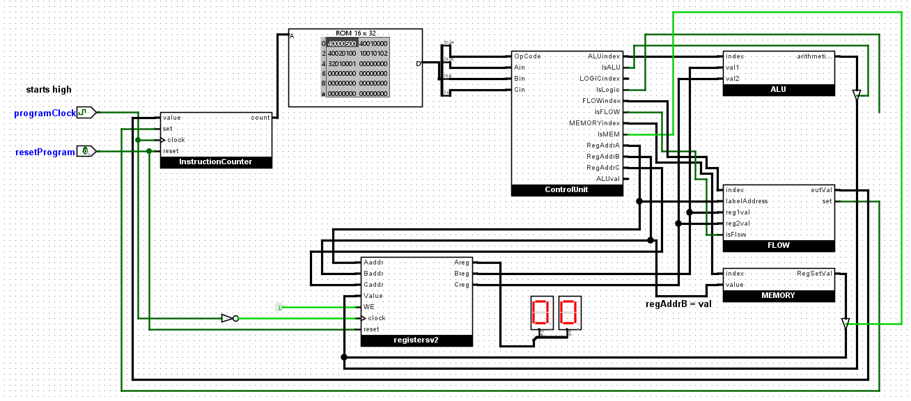
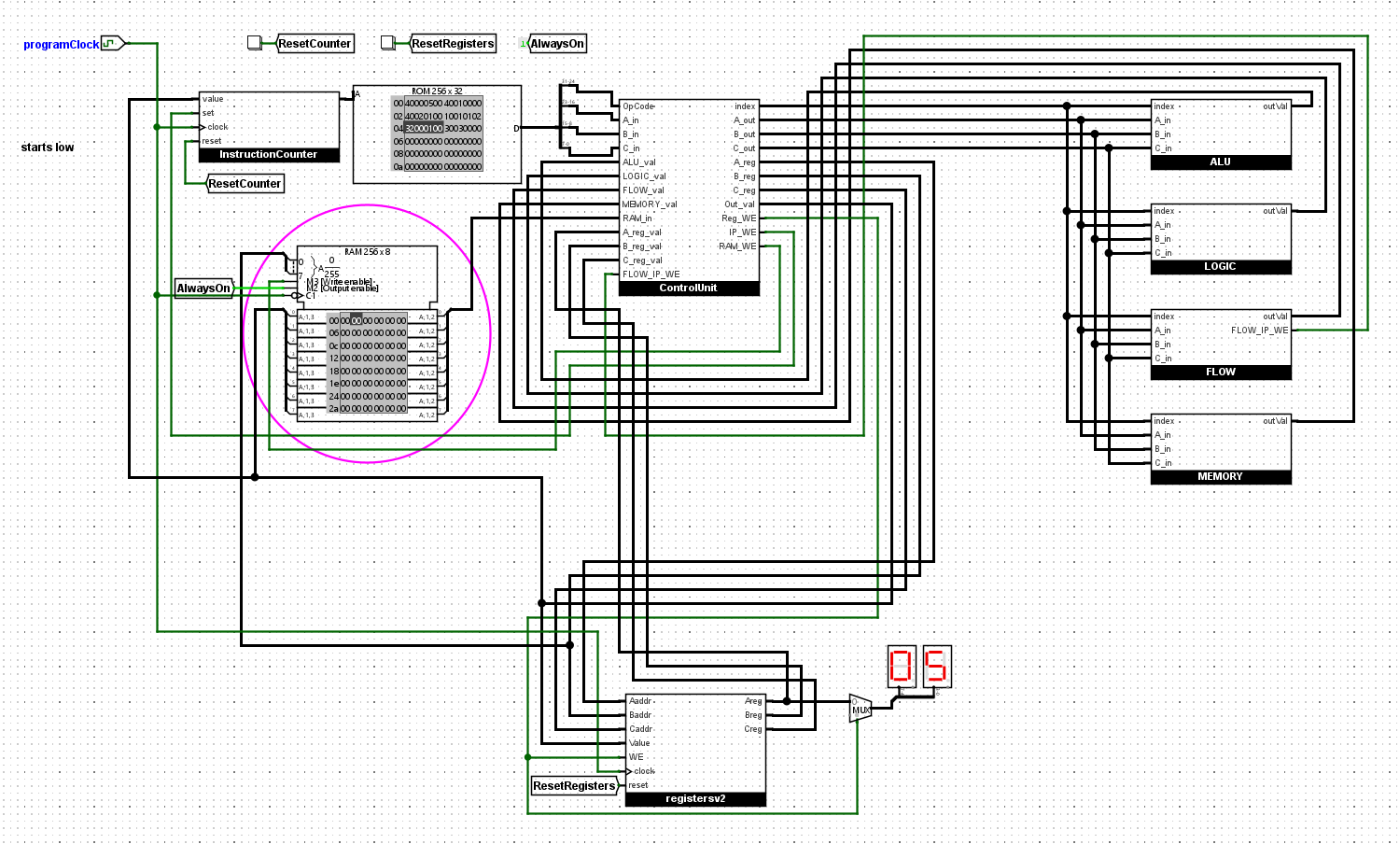
v1 worked, but each block (ALU, LOGIC, FLOW, MEMORY) decoded part of the instruction itself, so control signals got duplicated and buffered all over the sheet. In v2 one control unit reads the opcode and the three parameter fields and does all the routing in a single clock tick: it picks which block drives the register file and derives the three write enables (Reg_WE, IP_WE, RAM_WE).
That got rid of most of the control buffers, and it's what made RAM easy: LOAD and STR are just one more data source and one more write enable. The IP also went from 4 to 8 bits, so programs can be 256 instructions instead of 16. v2 is the base I'll extend for the stack.
v1: 16-word ROM, per-block decoding, 4-bit instruction counter.v2: 256-word ROM, central control unit, 256×8 RAM, 8-bit IP.
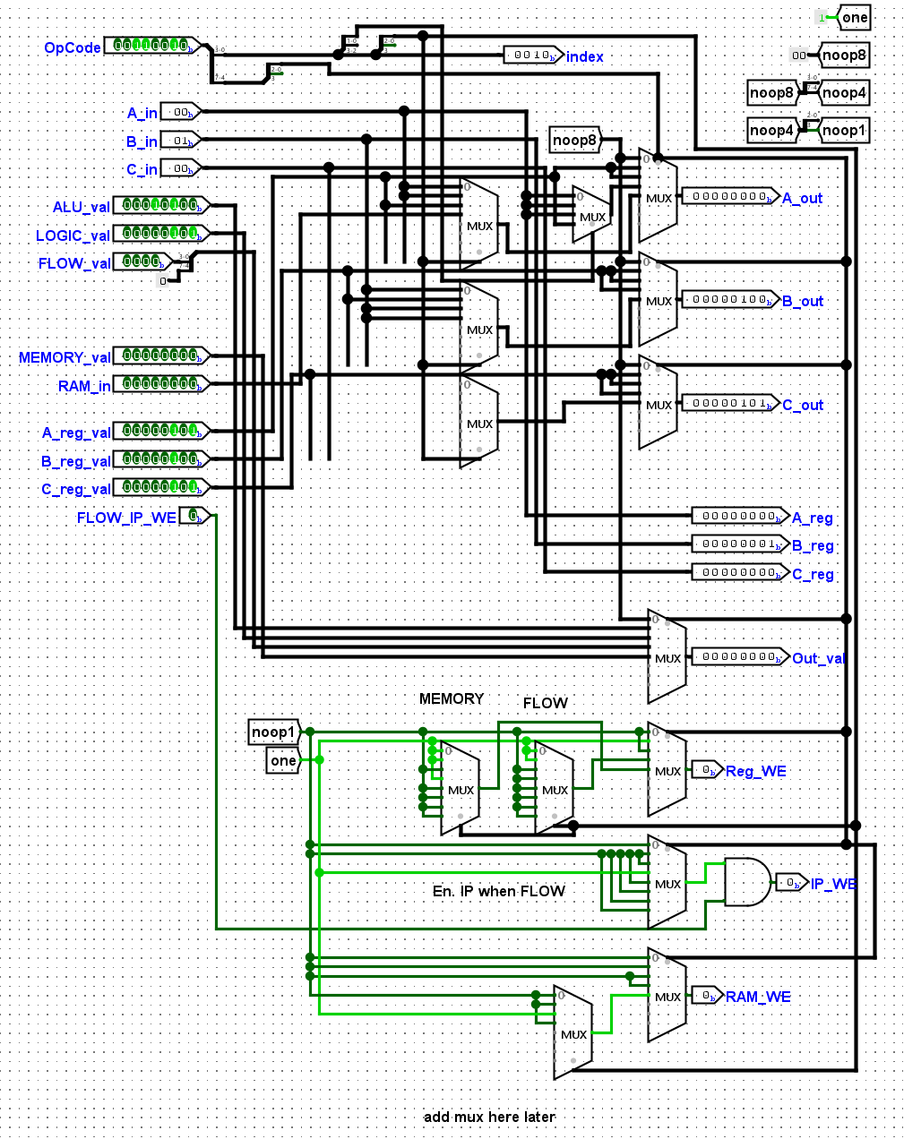
Inside the v2 control unit. The high nibble of the opcode picks ALU, LOGIC, FLOW or MEMORY, three muxes route the A/B/C register values to that block, and the green muxes at the bottom derive Reg_WE, IP_WE and RAM_WE from the same bits.
From simulation to breadboard
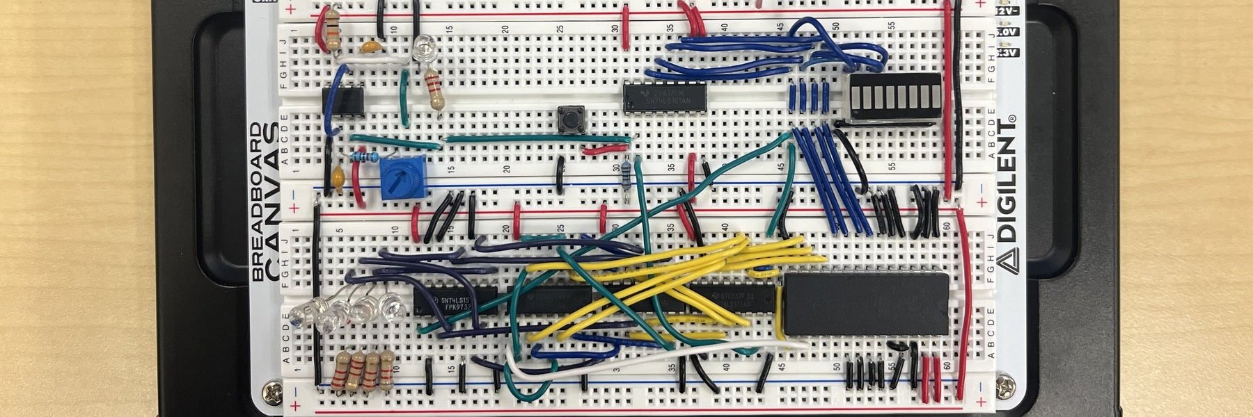
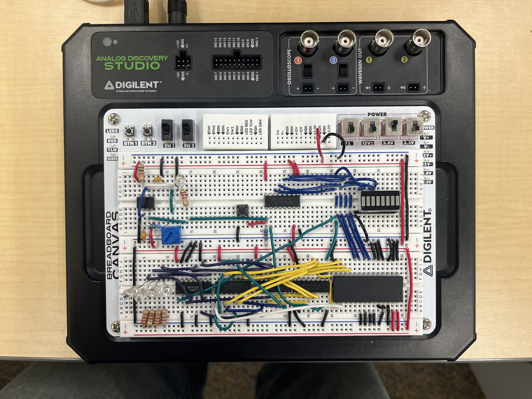
The full CPU has far too many gates to wire by hand, so I drew a much smaller circuit (logisim/logisim_small/simplercpu.circ): just the arithmetic core. It reads operands from ROM and runs them through a 2-to-1 mux, a 4-bit full adder and an XOR IC, enough for ADD and SUB. Once that worked in Logisim I built it with real 74LS chips on a Digilent breadboard, an AT28C256 EEPROM as the program ROM and an LED bar for the result.
Parts
AT28C256: 32K×8 parallel EEPROM, holds the program
Isolate the faulty instruction. When the CPU crashed on one instruction it was hard to see why mid-program. Running just that instruction and stepping the clock made most bugs obvious in a few ticks.
Write registers on the falling edge. v1 wrote registers on the rising edge, so within one tick a value could race out of a register, through the ALU and back in before anything settled. Writing on the falling edge gives the control unit and ALU the first half of the cycle to settle, and let me remove the NOT on the clock in the main circuit. I also put a mux on the register output so I don't see intermediate values between ticks.
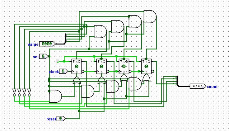
Build the IP as a register, not a counter. The v1 instruction pointer was a bunch of T flip-flops that didn't act the way they were supposed to, so I changed it to a register built from D flip-flops, which do.
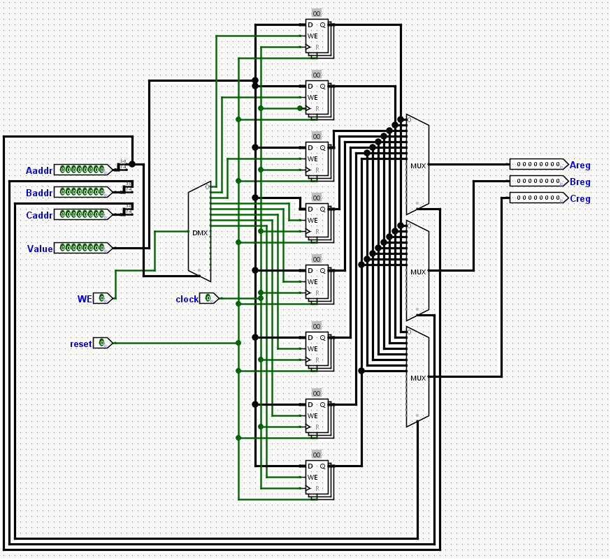
The v1 instruction counter: four T flip-flops plus the load logic.The register file: eight 8-bit registers behind a demux for writes and three muxes for the A, B and C read ports.
Testing the toolchain
There's an xUnit suite that GitHub Actions runs on every push. Every example program is assembled and compared byte-for-byte to its committed .bin, then disassembled and reassembled to check assemble(disassemble(bin)) == bin. There are also per-opcode encode/decode round trips and a label test (SET R0 5 / : TOP / JMP TOP has to give 30 01 00 00). The JavaScript emulator on this page was checked against the same binaries.
Rock Paper Scissors
A full game in SimpleISA. It asks RNDM for a 1–3 computer choice, spins on READ until a key shows up, echoes it with PRNT, maps r/p/s to 1/2/3, then walks the win table with EQ/JMPZ pairs and prints W, L or T. Pick it in the emulator above, click the console and type r, p or s. The listing below has the working-out comments trimmed; the file in the repo keeps them, including the block where I talk myself through which way JMPZ jumps.